- 您现在的位置:买卖IC网 > Sheet目录2000 > IDT5T9890NLI8 (IDT, Integrated Device Technology Inc)IC CLK DRIVER 2.5V PLL 68-VFQFPN
10
INDUSTRIALTEMPERATURERANGE
IDT5T9890
EEPROM PROGRAMMABLE 2.5V PROGRAMMABLE SKEW PLL CLOCK DRIVER
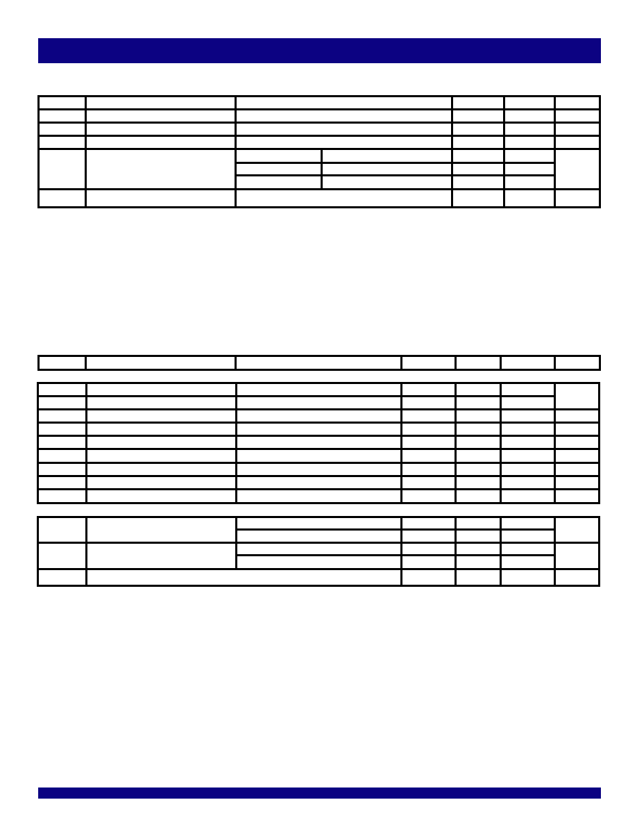
NOTE:
1. These inputs are normally wired to VDD, GND, or left floating. Internal termination resistors bias unconnected inputs to VDD/2. If these inputs are switched dynamically after powerup,
the function and timing of the outputs may be glitched, and the PLL may require additional tLOCK time before all datasheet limits are achieved.
DC ELECTRICAL CHARACTERISTICS OVER OPERATING RANGE
Symbol
Parameter
Test Conditions
Min.
Max
Unit
VIHH
Input HIGH Voltage Level(1)
3-Level Inputs Only
VDD – 0.4
—
V
VIMM
Input MID Voltage Level(1)
3-Level Inputs Only
VDD/2 – 0.2 VDD/2 + 0.2
V
VILL
InputLOWVoltageLevel(1)
3-Level Inputs Only
—
0.4
V
VIN = VDD
HIGH Level
—
200
I3
3-Level Input DC Current
VIN = VDD/2
MID Level
–50
+50
A
(ADDR0, ADDR1)
VIN = GND
LOW Level
–200
—
IPU
InputPull-UpCurrent
VDD = Max., VIN = GND
–100
—
A
DC ELECTRICAL CHARACTERISTICS OVER OPERATING RANGE FOR HSTL(1)
Symbol
Parameter
Test Conditions
Min.
Typ.(7)
Max
Unit
InputCharacteristics
IIH
Input HIGH Current
VDD = 2.7V
VI = VDDQN/GND
—
±5
A
IIL
InputLOWCurrent
VDD = 2.7V
VI = GND/VDDQN
——
±5
VIK
ClampDiodeVoltage
VDD = 2.3V, IIN = -18mA
—
- 0.7
- 1.2
V
VIN
DCInputVoltage
- 0.3
+3.6
V
VDIF
DCDifferentialVoltage(2,8)
0.2
—
V
VCM
DC Common Mode Input Voltage(3,8)
680
750
900
mV
VIH
DC Input HIGH(4,5,8)
VREF + 100
—
mV
VIL
DC Input LOW(4,6,8)
—VREF - 100
mV
VREF
Single-EndedReferenceVoltage(4,8)
—
750
—
mV
OutputCharacteristics
VOH
Output HIGH Voltage
IOH = -8mA
VDDQN - 0.4
—
V
IOH = -100
AVDDQN - 0.1
—
VOL
OutputLOWVoltage
IOL = 8mA
—
0.4
V
IOL = 100
A
—
0.1
VOX
FB/FB Output Crossing Point
VDDQN/2 - 150
VDDQN/2
VDDQN/2 + 150
mV
NOTES:
1. See RECOMMENDED OPERATING RANGE table.
2. VDIF specifies the minimum input differential voltage (VTR - VCP) required for switching where VTR is the "true" input level and VCP is the "complement" input level. Differential mode
only. The DC differential voltage must be maintained to guarantee retaining the existing HIGH or LOW input. The AC differential voltage must be achieved to guarantee switching
to a new state.
3. VCM specifies the maximum allowable range of (VTR + VCP) /2. Differential mode only.
4. For single-ended operation, in differential mode, REF[1:0]/VREF[1:0] is tied to the DC voltage VREF[1:0].
5. Voltage required to maintain a logic HIGH, single-ended operation in differential mode.
6. Voltage required to maintain a logic LOW, single-ended operation in differential mode.
7. Typical values are at VDD = 2.5V, VDDQN = 1.5V, +25°C ambient.
8. The reference clock input is capable of HSTL, eHSTL, LVEPECL, 1.8V or 2.5V LVTTL operation independent of the device output. (See Input/Output Selection table.)
发布紧急采购,3分钟左右您将得到回复。
相关PDF资料
IDT5V19EE604NDGI8
IC PLL CLK GEN 200MHZ 28VFQFPN
IDT5V40501DVG
IC CLK GEN PLL 160MHZ 8TSSOP
IDT5V41064NLGI
IC CLK GEN 1:1 16QFN
IDT5V41066PGG
IC CLK GEN SPRED SPECTRM 20TSSOP
IDT5V49EE901NLGI8
IC PLL CLK GEN 200MHZ 32VFQFN
IDT5V49EE902NLGI
IC CLOCK GEN PLL 500MHZ 32VFQFPN
IDT5V49EE904NLGI8
IC PLL CLK GEN 200MHZ 32VFQFN
IDT821024PPG
IC PCM CODEC QUAD NONPROG 44TQFP
相关代理商/技术参数
IDT5T9891NLGI
功能描述:IC CLK DRIVER 2.5V PLL 68-VFQFPN RoHS:是 类别:集成电路 (IC) >> 时钟/计时 - 时钟发生器,PLL,频率合成器 系列:- 标准包装:39 系列:- 类型:* PLL:带旁路 输入:时钟 输出:时钟 电路数:1 比率 - 输入:输出:1:10 差分 - 输入:输出:是/是 频率 - 最大:170MHz 除法器/乘法器:无/无 电源电压:2.375 V ~ 3.465 V 工作温度:0°C ~ 70°C 安装类型:* 封装/外壳:* 供应商设备封装:* 包装:*
IDT5T9891NLGI8
功能描述:IC CLK DRIVER 2.5V PLL 68-VFQFPN RoHS:是 类别:集成电路 (IC) >> 时钟/计时 - 时钟发生器,PLL,频率合成器 系列:- 标准包装:39 系列:- 类型:* PLL:带旁路 输入:时钟 输出:时钟 电路数:1 比率 - 输入:输出:1:10 差分 - 输入:输出:是/是 频率 - 最大:170MHz 除法器/乘法器:无/无 电源电压:2.375 V ~ 3.465 V 工作温度:0°C ~ 70°C 安装类型:* 封装/外壳:* 供应商设备封装:* 包装:*
IDT5T9891NLI
功能描述:IC CLK DRIVER 2.5V PLL 68-VFQFPN RoHS:否 类别:集成电路 (IC) >> 时钟/计时 - 时钟发生器,PLL,频率合成器 系列:- 标准包装:39 系列:- 类型:* PLL:带旁路 输入:时钟 输出:时钟 电路数:1 比率 - 输入:输出:1:10 差分 - 输入:输出:是/是 频率 - 最大:170MHz 除法器/乘法器:无/无 电源电压:2.375 V ~ 3.465 V 工作温度:0°C ~ 70°C 安装类型:* 封装/外壳:* 供应商设备封装:* 包装:*
IDT5T9891NLI8
功能描述:IC CLK DRIVER 2.5V PLL 68-VFQFPN RoHS:否 类别:集成电路 (IC) >> 时钟/计时 - 时钟发生器,PLL,频率合成器 系列:- 标准包装:39 系列:- 类型:* PLL:带旁路 输入:时钟 输出:时钟 电路数:1 比率 - 输入:输出:1:10 差分 - 输入:输出:是/是 频率 - 最大:170MHz 除法器/乘法器:无/无 电源电压:2.375 V ~ 3.465 V 工作温度:0°C ~ 70°C 安装类型:* 封装/外壳:* 供应商设备封装:* 包装:*
IDT5T989X-982X-M1
功能描述:KIT FOR 5T989X-982X RoHS:否 类别:编程器,开发系统 >> 评估演示板和套件 系列:- 标准包装:1 系列:- 主要目的:电信,线路接口单元(LIU) 嵌入式:- 已用 IC / 零件:IDT82V2081 主要属性:T1/J1/E1 LIU 次要属性:- 已供物品:板,电源,线缆,CD 其它名称:82EBV2081
IDT5T9950APFGI
功能描述:IC CLK BUFFER/DVR 1:10 32TQFP RoHS:是 类别:集成电路 (IC) >> 时钟/计时 - 时钟发生器,PLL,频率合成器 系列:TurboClock™ II JR 标准包装:1,000 系列:- 类型:时钟/频率合成器,扇出分配 PLL:- 输入:- 输出:- 电路数:- 比率 - 输入:输出:- 差分 - 输入:输出:- 频率 - 最大:- 除法器/乘法器:- 电源电压:- 工作温度:- 安装类型:表面贴装 封装/外壳:56-VFQFN 裸露焊盘 供应商设备封装:56-VFQFP-EP(8x8) 包装:带卷 (TR) 其它名称:844S012AKI-01LFT
IDT5T9950APFGI8
功能描述:IC CLK BUFFER/DVR 1:10 32TQFP RoHS:是 类别:集成电路 (IC) >> 时钟/计时 - 时钟发生器,PLL,频率合成器 系列:TurboClock™ II JR 标准包装:1,000 系列:- 类型:时钟/频率合成器,扇出分配 PLL:- 输入:- 输出:- 电路数:- 比率 - 输入:输出:- 差分 - 输入:输出:- 频率 - 最大:- 除法器/乘法器:- 电源电压:- 工作温度:- 安装类型:表面贴装 封装/外壳:56-VFQFN 裸露焊盘 供应商设备封装:56-VFQFP-EP(8x8) 包装:带卷 (TR) 其它名称:844S012AKI-01LFT
IDT5T9950PFGI
功能描述:IC CLK BUFFER/DVR 1:10 32TQFP RoHS:是 类别:集成电路 (IC) >> 时钟/计时 - 时钟发生器,PLL,频率合成器 系列:TurboClock™ II JR 标准包装:2,000 系列:- 类型:PLL 频率合成器 PLL:是 输入:晶体 输出:时钟 电路数:1 比率 - 输入:输出:1:1 差分 - 输入:输出:无/无 频率 - 最大:1GHz 除法器/乘法器:是/无 电源电压:4.5 V ~ 5.5 V 工作温度:-20°C ~ 85°C 安装类型:表面贴装 封装/外壳:16-LSSOP(0.175",4.40mm 宽) 供应商设备封装:16-SSOP 包装:带卷 (TR) 其它名称:NJW1504V-TE1-NDNJW1504V-TE1TR